- Description
- Brand
Description

DLP is the abbreviation of "Digital Light Procession", that is, digital light processing, which means that this technology first digitally processes the image signal and then projects the light.
At the heart of every DLP chipset is a highly reflective aluminum micromirror array, known as a digital micromirror device (DMD). DMD is an electronically input, optically-output microelectromechanical system (MEMS) that enables developers to perform high-speed, efficient, and reliable spatial light modulation. Using TI's proven semiconductor production technology, each DMD contains up to 800 million independently controlled micromirrors built on the corresponding CMOS memory cell.
During operation, the DMD controller loads a "1" or a "0" for each base memory unit. This is followed by the application of a lens reset pulse, which causes each micromirror to deviate electrostatically by approximately one hinge, resulting in a corresponding +/-° state. The deviation angle of these two valid states is repeatable due to the physical stop caused by the resistance of the two spring ejectors.
| DMD micromirror array | Transfer speed | ||||||||
|---|---|---|---|---|---|---|---|---|---|
| Model | DMD | wavelength | array | Pixels/μm | Mirror/mm | 1bit | CPU | Data transfer rate | port |
| D6500 | 0.65" | VIS | 1920 x 1080 | 7.6 | 14.5x8.2 | 9253 | 400MHz | 25.6Gb/s | USB2.0 |
| D4100-0.55 XGA | 0.55" | VIS | 1024 x 768 | 10.8 | 11.0x8.3 | 32552 | 400MHz | 25.6Gb/s | USB2.0 |
| D4100-0.7 XGA | 0.7" | VIS,UV,NIR | 1024 x 768 | 13.7 | 14.0x10.5 | 32552 | 400MHz | 25.6Gb/s | |
| D4100-0.95 1080p | 0.95" | VIS,UV | 1920 x 1080 | 10.8 | 20.7x11.7 | 23148 | 400MHz | 51.2Gb/s | |
| The D4100 integrates Texas Instruments' 2xLVDS DLP set with Xilinx's Virtex 5 chip to maximize the performance benefits of the 2xLVDS DLP set. | |||||||||
| Support USB 2.0 high-speed picture transmission and display, with internal and external synchronous trigger function; Provide USB 2.0 underlying driver and dynamic link library files to facilitate secondary development; | |||||||||
| D4200-0.55 XGA | 0.55" | VIS | 1024 x 768 | 10.8 | 11.0x8.3 | 32552 | 400MHz | 25.6Gb/s | Gigabit Ethernet (X2) |
| D4200-0.7 XGA | 0.7" | VIS,UV,NIR | 1024 x 768 | 13.7 | 14.0x10.5 | 32552 | 400MHz | 25.6Gb/s | Gigabit Fiber (X2) |
| D4200-0.95 1080p | 0.95" | VIS,UV | 1920 x 1080 | 10.8 | 20.7x11.7 | 23148 | 400MHz | 51.2Gb/s | 1 Gigabit Fiber (X<>) |
| The D4200 upgrades the original D4100 from one DDR2 memory module to two DDR2 memory modules, and the USB 3.2 interface to Gigabit Ethernet (X0), Gigabit Fiber (X2) and 2,1 Gigabit Fiber (X<>), further improving system data throughput and maximizing DMD performance. | |||||||||
Technical advantages:
- Support 0.95, 0.7, 0.55 resolution DMD;
- Support high-speed picture transmission of Gigabit Ethernet, Gigabit fiber, 10,000 Gigabit fiber, and have internal and external synchronous trigger functions;
- Provide Gigabit Ethernet, PCIE board underlying driver and dynamic link library files to facilitate secondary development;
- Support USB 2.0 high-speed picture transmission and display, with internal and external synchronous trigger function;
- Provide USB 2.0 underlying driver and dynamic link library files to facilitate secondary development;
- Support XGA and 1080P resolution single micromirror precise control and locking;
- Contrast ratio over 2000:1;
- Support band range from 350nm-2700nm (different DMD);
- The micromirror is locked at any time;
- The binary flip frequency of the micromirror can be set.
Fields of application:
- 3D measurement, 3D scanning
- Intelligent display, virtual reality
- Machine vision, machine placement
- Spectral analysis, chemical analysis
- Quality inspection, surface inspection
- Biological microscopy, microscopic imaging
- Medical measurement, dental measurement
- PCB exposure, 3D printing
- Vascular scintigraphy, biometrics
- Scene generation, optical networking, etc
Application areas

3D printing
3D printing technology is a kind of rapid prototyping technology, which is a technology based on mathematical model files, using adhesive materials such as powdered metal or plastic, and constructing objects layer by layer. It is often used in mold manufacturing, industrial design and other fields to manufacture models, and then gradually used in the direct manufacture of some products, and there are already parts printed using this technology. The technology has applications in jewelry, footwear, industrial design, architecture, engineering and construction (AEC), automotive, aerospace, medical industry, education, geographic information systems, civil engineering, firearms, and other fields.

spectroscopic analysis
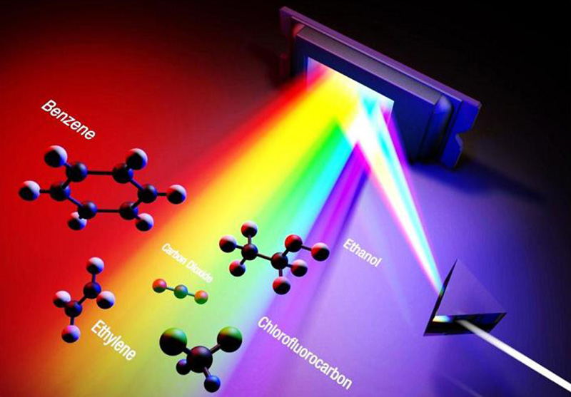
Spectroscopy is a powerful non-contact technique that can quickly identify the composition and associated properties of substances by analyzing changes in absorption or reflection of light at different wavelengths throughout the spectrum. Spectral analysis according to the spectrum of the substance to identify the substance and determine its chemical composition and relative content, according to the principle of analysis, spectrum analysis can be divided into emission spectrum analysis and absorption spectrum analysis two types. Spectral analysis can support visible, IR, or UV wavelengths.

3D machine vision
3D detection is a fast and accurate way to collect physical information of objects, through the processing of images and data, you can obtain the length, width, height, volume, feature size, feature position, area and other information of the object.
DLP spatial light modulation technology has many application cases in the medical field, such as: phototherapy laser treatment, ophthalmology, vascular projection, skin measurement, genetic science, etc.

Digital exposure
Photolithography is an important step in the semiconductor device manufacturing process that uses exposure and development to characterize the geometric structure on the photoresist layer, and then transfer the pattern on the photomask to the substrate by etching. The substrate here contains not only silicon wafers, but also other metal layers, dielectric layers, such as glass, sapphires in SOS.

Infrared simulation
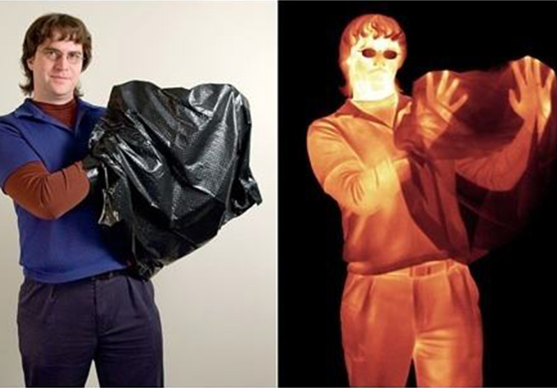
Scene infrared simulation can be applied to infrared image analysis research, battlefield environment simulation and infrared weapon testing and many other fields. The image is compressed into a single pixel by compression technology and special coding, and then the image is obtained remotely by the infrared emitting / receiving device, and the captured picture is obtained by decoding.

Compression sensing
First, the imaging target is projected onto the DMD through the optical path system, and the reflected light is focused by the lens to a single photodiode, and the voltage value at both ends of the photodiode is a measured value X, and the projection operation is repeated N times, and then the original image is constructed by the algorithm.
DMD is controlled by a digital voltage signal to flip the microlens to adjust the incident light, which is equivalent to a 0-1 random measurement matrix.


